
Jama Software is always looking for news that would benefit and inform our industry partners. As such, we’ve curated a series of customer and industry spotlight articles that we found insightful. In this blog post, we share an article from EE Times, titled “Strategies for Addressing More Complex Custom Chip Design”, and written by Abhishek Jadhav and published on March 21, 2025.
Strategies for Addressing More Complex Custom Chip Design
Unprecedented growth and demand for edge computing and high-performance computing (HPC) is creating new opportunities and significant challenges for custom chips. We spoke to Sondrel CEO Oliver Jones to discuss some of the approaches to addressing these needs.
Custom chip design is a multifaceted process involving many considerations, from power efficiency and performance trade-offs to manufacturing and packaging complexities. One of the primary challenges in this domain is managing power, performance and area (PPA) trade-offs.
Designers must carefully balance these factors to ensure that the final product meets the strict requirements of modern applications like AI at the edge or HPC workloads. Additionally, the process involves navigating geopolitical disruptions and supply chain constraints, which can delay production and increase costs.
Startups and established companies also face hurdles like limited resources, lack of access to advanced manufacturing facilities and navigating the intricate supply chain required for production. The role of specialized ASIC suppliers is to offer expertise in balancing power efficiency, managing supply chains and streamlining production.
“Selecting a turnkey supplier to handle a complete ASIC project is much more challenging than selecting an ASIC design house. There needs to be a high level of confidence and trust,” Jones said.
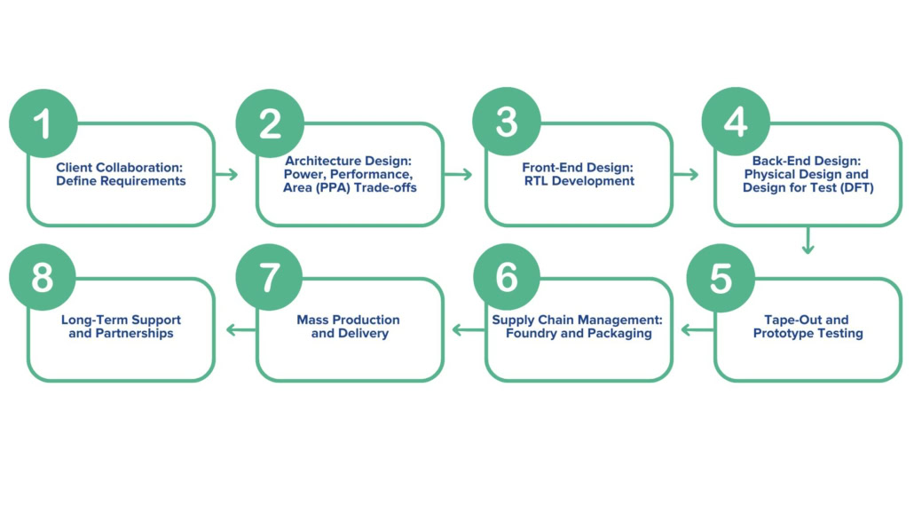
Flowchart explaining the turnkey model. (Inspired by source Sondrel)
In response to these challenges, some companies have adopted the turnkey model, which manages every stage of chip development—from initial concept to mass production. This approach simplifies the process for clients, especially startups lacking the resources or expertise to develop custom chips independently. By integrating services like architecture design, physical design and design for testing, turnkey providers reduce the risks and complexities associated with chip production.
For example, a turnkey provider’s partner ecosystem, including foundries like TSMC and GlobalFoundries, ensures a smooth transition from design to manufacturing. “Startups often have fantastic ideas but lack the capability and resources to translate them into hardware. We’re selective about who we work with, allowing us to provide closer attention and better service to each customer,” Jones explained.
RELATED: Buyer’s Guide: Selecting a Requirements Management and Traceability Solution for Semiconductor
Case study: AI at the edge
In one example, a U.S.-based AI startup specializing in image and video recognition technology needed to develop an AI accelerator chip for edge applications, such as surveillance and facial recognition. This required a custom design to address challenges in architecture, packaging and supply chain management—areas particularly daunting for a startup with limited resources.
For this project, Sondrel helped the startup identify the need for a flip-chip CSP package with an ultra-low profile of 2.5 millimeters to meet the space and performance constraints. By pre-booking packaging slots, the lead time was reduced from 42 weeks to 12–16 weeks, accelerating the product’s time-to-market. The project integrated the startup’s proprietary AI IP to deliver a reliable and efficient chip that became central to the startup’s AI accelerator hardware.
By leveraging the provider’s ecosystem and expertise, the startup successfully developed a 16-nm FinFET chip in just two years.
The role of turnkey custom chip design houses
Startups face unique challenges in custom chip design, often struggling to access the resources and expertise needed to bring their ideas to life. Resource constraints can make it difficult to define optimal PPA trade-offs or secure manufacturing capacity. Additionally, supply chain disruptions, whether due to geopolitical tensions or market volatility, can create significant hurdles.
Edge AI applications, such as autonomous vehicles, smart cities and IoT devices, require custom chips capable of processing large amounts of data locally while minimizing power consumption. Similarly, HPC workloads, including scientific simulations and big data analytics, demand chips optimized for performance and scalability.
“AI at the edge and HPC are where we see the strongest demand,” Jones said.
Considering the rapidly evolving landscape, collaboration among design houses, foundries and ecosystem partners is critical. The ability to integrate advanced process nodes, innovative packaging solutions and robust supply chain strategies will define the future of custom chip design.
To address these issues, turnkey providers have developed foundry-agnostic approaches that offer greater flexibility. These approaches involve designing chips in a way that can be manufactured across different foundries without being tied to a single supplier, allowing companies to adapt to changing manufacturing capacities and avoid bottlenecks.
By maintaining strong relationships with multiple foundries, providers can secure wafer allocations and advanced packaging solutions, reducing lead times and minimizing risks. Selecting the right kind of chip packaging plays a key role here, and turnkey providers help companies to adopt the latest and innovative packaging solutions.
RELATED: Traceable Agile™ – Speed AND Quality Are Possible for Software Factories in Safety-critical Industries
Advanced packaging and open source add to the mix
While turnkey models provide a valuable solution, other strategies are also emerging to address the challenges of custom chip design. Collaborative research initiatives and public-private partnerships are playing an increasingly important role in driving innovation. For example, government-backed programs in Europe and North America are funding projects aimed at developing next-generation semiconductors.
Open-source hardware initiatives are another promising avenue. By providing a shared foundation for chip design, these initiatives can lower costs and accelerate development timelines—particularly for startups. Additionally, advancements in design automation tools are making it easier for companies to optimize PPA trade-offs and streamline the development process.
Innovative packaging solutions are a critical component of modern chip design, enabling manufacturers to achieve higher levels of integration and performance. Techniques like flip-chip and wafer-level packaging are becoming increasingly popular for applications in edge AI and HPC.
Flip-chip packaging allows direct electrical connections between the chip and the substrate, reducing signal interference and improving thermal management. Wafer-level packaging, on the other hand, integrates the packaging process directly on the wafer, enabling a smaller form factor, improved performance and lower production costs. These methods not only improve performance but also reduce the overall size and power consumption of chips.
For instance, in the aforementioned case study, using a flip-chip CSP package with an ultra-low profile of 2.5 millimeters significantly reduced lead times and enhanced the chip’s performance. This example underscores the importance of packaging innovations in meeting the demands of next-generation applications.
As edge computing and HPC continue to grow, the demand for custom chip design will only increase. The future of the semiconductor industry will be shaped by advancements in process technology, innovative packaging solutions and collaborative ecosystems. Companies that can effectively address the challenges of custom chip development will be well-positioned to lead in this dynamic market.
To achieve this, industry stakeholders must prioritize collaboration, investing in partnerships that span design, manufacturing and supply chain management. By working together, they can overcome the barriers to entry and accelerate the development of chips that power the next wave of technological innovation.
The custom chip design process is a testament to the complexity and ingenuity required to meet the demands of edge AI and HPC. Through a combination of innovative strategies and collaborative efforts, the industry is redefining what is possible, paving the way for a future where technology continues to push the boundaries of performance and efficiency.
Subject matter experts from Jama Software provide guidance and best practices on requirements management, test management, compliance and regulation, risk management, and complex product and software development.
Latest posts by Jama Software (see all)