In today’s competitive markets, every second counts to meet strict project timelines. OrCAD X Presto contains technology which enhances design productivity, including the search panel. The search panel provides an easy-to-use interface to search, filter, edit, and locate any object in the design. Designers can use the search panel to accelerate PCB design tasks including:
- Placing components
- Locating specific objects
- Editing design parameters in bulk
- Complete unrouted connections
- Find and fix design rule violations
This quick how-to will provide step-by-step instructions on how to use the search panel in OrCAD X Presto.
To follow along, download the provided files above the table of contents.
How-To Video
 Open in New Window
Use the Search Panel to Place Components
Note: The search panel can be used to quickly locate and place the desired components on the PCB.
Step 1: Open the provided design, presto_tutorial.brd, in OrCAD X Presto.
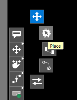
Step 2: Right-click the move icon on the toolbar and select the Place.
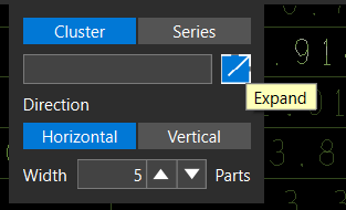
Step 3: In the Place Component pop-up ensure Cluster is set as the placement type and Horizontal with a width of 5 is selected as the Direction. Select Expand.
Step 4: The search panel opens at the bottom of the OrCAD X Presto canvas displaying the components in the design. Select the Filter icon for the State to activate the filtering options.
Step 5: Select the Filter icon again. From the State drop-down menu check Unplaced. Click to select a blank spot in the filter pop-up window and click OK.
Step 6: Only the unplaced components are now displayed in the search panel. Click and drag to highlight all the components listed.
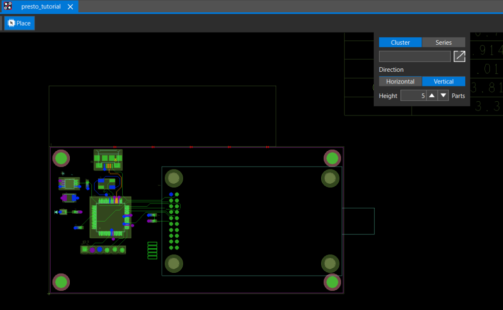
Step 7: Move your cursor into the PCB canvas. The components are arranged in a horizontal line. Change the direction to Vertical in the placement window.
Step 8: Click to place the components in the PCB canvas then select the arrow icon on the toolbar.
Use the Search Panel to Locate Design Objects
Note: The search panel can also be used to quickly locate any object in the design. If the search panel was closed, it can be activated by selecting View > Panels > Search from the menu.
Step 9: Select the tab for the search panel at the bottom of the OrCAD X Presto canvas and select the Reset Filter button to clear the previous search.
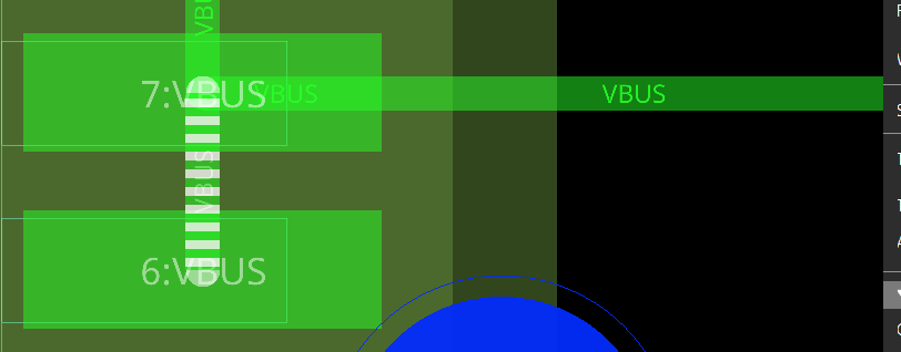
Step 10: In the Search bar, type USB and press Enter to search.
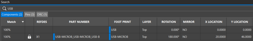
Step 11: View the results. A mechanical model of a USB device and the USB placed on the PCB have been identified and reported. Verify the X and Y location of the PCB component is configured as 20 and 46 respectively.
Step 12: Select the lock icon to lock the component in place to prevent accidental moving.
Step 13: Delete USB from the search bar and click Enter on the keyboard to clear the search.
Use the Search Panel to Bulk Edit Design Parameters
Note: The search panel can be used to locate aspects of the design and edit parameters in bulk, minimizing mouse clicks and saving time.
Step 14: Select the Traces/Wires tab in the search panel. This will display all traces in the PCB design.
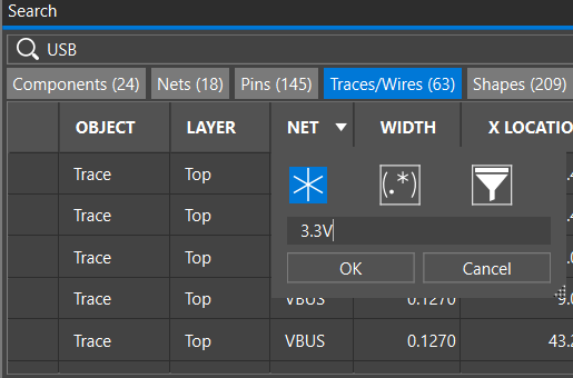
Step 15: Select the Filter icon for the Net category. Ensure the wildcard search is selected and type 3.3V into the search field. Select OK.
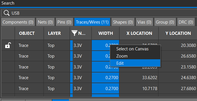
Step 16: The nets have been filtered to show only the 3.3V nets. Click and drag the values in the width column. Right-click and select Edit.
Step 17: Type 0.381 as the value and press Enter on the keyboard. All the trace width values have been changed for the 3.3V nets in the search panel and within the design.
Step 18: Select the Reset Filter button within the search panel.
Use the Search Panel to Complete a Design
Note: The search panel can be used to quickly locate and resolve unplaced components, unrouted nets, and unrouted connections to efficiently complete your PCB designs.
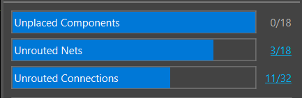
Step 19: In the Properties Panel in the OrCAD X Presto canvas, view the design status containing the unplaced components, unrouted nets, and unrouted connections. Select Unrouted Connections.
Step 20: The search panel is populated with all the unrouted connections in the design. Double-click the first entry, pin C4.1, to be brought to the location on the PCB.
Step 21: Adjust the PCB canvas using the – key on the keyboard to zoom out and the arrow keys to pan the view. The capacitors that were placed earlier in this how-to have not been routed.
Step 22: Right-click on the Add Connect icon on the toolbar and select Fanout.
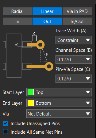
Step 23: In the Fanout pop-up window, select Linear and Out for the fanout configuration. Select a blank area of the PCB canvas to deselect the C4.1 pin.
Step 24: Click to select each of the unrouted capacitors (C4, C5, C6, C7, and C8). Select the Arrow icon from the toolbar then click a blank space in the PCB canvas.
Step 25: View the design status in the properties panel. There is still an unrouted connection. Click the hyperlink for the Unrouted Connection to expand the search panel and display the result.
Step 26: The two pins which need to be connected are displayed. Double-click one of the pins to be brought to the location on the PCB canvas.
Step 27: Adjust the PCB canvas using the – key on the keyboard to zoom out and the arrow keys to pan the view.
Step 28: Right-click the fanout icon on the toolbar and select Add Connect.
Step 29: Click to select pin U1.7 then click to select pin U1.6 to complete the connection.
Step 30: Select the Arrow key from the toolbar then select a blank area in the PCB canvas.
Use the Search Panel to Correct Errors
Note: The search panel can be used to quickly filter, locate, and fix design rule errors to ensure your design meets the defined specifications and requirements.
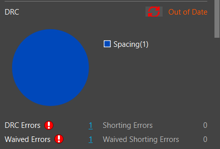
Step 31: View the properties panel in the PCB canvas to review the Design Rule Check (DRC) errors. The DRC is out-of-date. Select the Refresh symbol for Out of date shapes.
Step 32: There is one DRC error listed and one DRC error that has been waived already. Select the pie chart or the hyperlinked DRC error to view the error.
Note: There may be other DRC errors listed depending on the placement of capacitors C4-C8. If this occurs, select the Spacing DRC portion of the pie chart.
Step 33: Double-click the entry listed in the search panel to be brought to the location on the PCB canvas. The DRC error is flagged with a DRC marker. Adjust the PCB canvas using the – key on the keyboard to zoom out and the arrow keys to pan the view as needed.
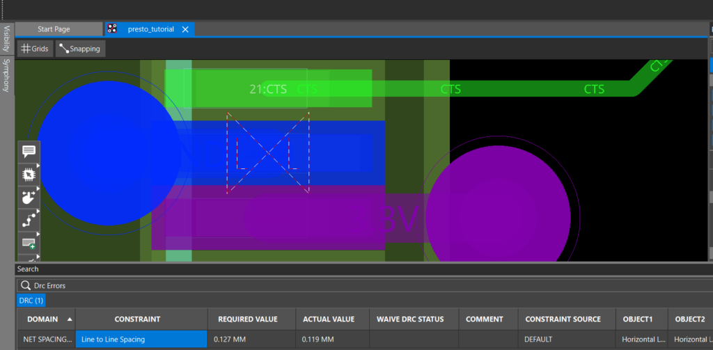
Step 34: This DRC error is reporting insufficient spacing between the ground trace and the 3.3V trace due to the pin pitch of the IC. For this example, we will decrease the trace width of the ground net. Click to select the trace for the ground net.
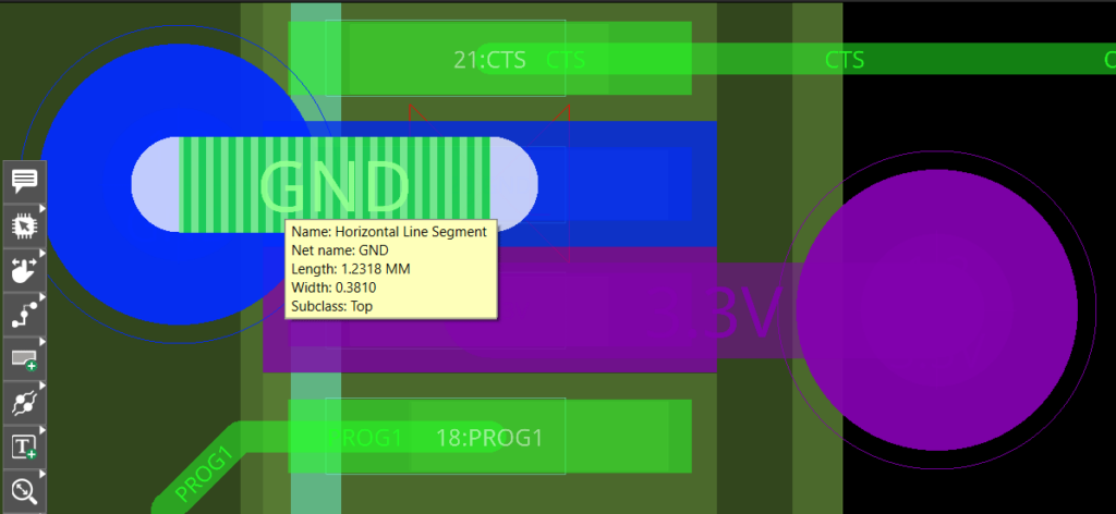
Step 35: In the properties panel, adjust the trace width to 0.280 and click Enter on the keyboard.
Step 36: Click a blank area in the PCB canvas. The DRC error is resolved.
Wrap Up & Next Steps
Use the search panel to efficiently complete various tasks throughout your PCB design process with the powerful global search and filtering functionality in OrCAD X Presto. Test out this feature and more with a free trial of OrCAD X. Get more step-by-step instructions for OrCAD X Presto and a walk-through course to jumpstart your PCB designs at EMA Academy.
