
Resolving the Signal Part 6: The Effects of Amplifier Noise on Delta-Sigma ADCs
Part 6 of this 12-part Resolving the Signal series focuses on output- versus input-referred noise, adding an amplifier at the input of an ADC, and low- versus high-resolution ADCs as they relate to amplifier noise.
This 12-part article series focuses on the impact of noise in delta-sigma ADCs. Part 6 of the Resolving the Signal series focuses on output- versus input-referred noise, adding an amplifier at the input of an ADC, and low- versus high-resolution ADCs as they relate to amplifier noise.
In many data acquisition (DAQ) systems, taking precision measurements of low-level input signals is a common design challenge. For example, many factory automation applications use programmable logic controllers (PLCs) to make decisions based on temperature sensor or load cell readings. Similarly, oil-drilling platforms use industrial differential-pressure flow meters to determine — with milliliter precision — how much oil is removed from a well.
To measure these process variables, many types of end equipment employ analog sensors such as resistance temperature detectors (RTDs), thermocouples or resistive bridges. These sensors typically output very low-level signals that need to be gained up above the DAQ system’s noise floor. Additionally, engineers may use gain to increase dynamic range by using more of the analog-to-digital converter’s (ADC) full-scale range (FSR). In either case, adding gain to any analog system generally requires an amplifier, which may be a discrete component or integrated into one of the signal-chain components, such as an ADC.
As with the introduction of any component to an electrical system, these amplifiers contribute noise. How does this noise affect the system? Parts 6 and 7 of the “Resolving the Signal” article series seek to answer this question by offering an in-depth understanding of amplifier noise and how it affects a typical signal chain.
Part 6 focuses on these topics as they relate to amplifier noise:
- Output- vs. input-referred noise.
- Adding an amplifier at the input of an ADC.
- Low- vs. high-resolution ADCs.
Part 5 continued to explore effective noise bandwidth as it relates to delta-sigma ADCs and system-level design. Part 7 will offer a detailed design example using commercially available ADCs and amplifiers to complement and expand on the theories explored in this article.
Output- vs. Input-Referred Noise
Output-referred noise — or noise referred-to-output, VN,RTO — is the noise measured at the output of the ADC, as its name implies. Recall from part 2 of this series that one method ADC manufacturers use to characterize ADC noise is to short the device’s inputs together and measure the noise at the output to determine the intrinsic noise of the ADC, as shown in Figure 1.
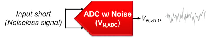
Figure 1. Measuring output-referred noise
However, also recall that the value actually reported in the data sheet is typically input-referred. Similar to output noise, input-referred noise — or noise referred-to-input, VN,RTI — is the noise at the input of the ADC. Unlike output-referred noise, input-referred noise is calculated, not measured. For an ADC with no integrated gain stage, the input-referred noise is equal to the output-referred noise, as shown in Equation 1:
Equation 1
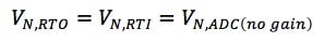
Why do ADC manufacturers specify noise as input-referred rather than output-referred? To answer this question, it helps to create an equivalent circuit noise model by separating the ADC from its noise into a “noiseless” ADC, preceded by a voltage source equal to the ADC’s input-referred noise, as shown in Figure 2.
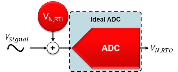
Figure 2. Noiseless ADC preceded by a noise source equal to the ADC's input-referred noise
Now, when you input a real signal into the ADC, it’s easy to see that you want ADC noise to be characterized as input-referred because this defines the system’s input resolution. Effectively, the input signal “competes” with the input-referred noise: If the signal’s amplitude is greater than the input-referred noise, you will be able to observe it; otherwise, the signal will be buried in the noise and you won’t be able to observe it.
Ultimately, if you know the smallest input signal you need to resolve, the input-referred noise tells you very quickly and easily if a specific ADC can provide the necessary resolution. And while this is less important for stand-alone ADCs where output-referred noise is equal to input-referred noise, what happens if you add an amplifier into the signal path?
Adding an Amplifier to the Input of an ADC
To analyze the amplifier’s impact on overall system noise, you can separate it from its noise source just as you did for the ADC. In this case, you can model it as a noiseless amplifier preceded by a voltage source equal to the amplifier’s noise, VN,AMP, shown in Figure 3. Additionally, you can assume that the input source (VSIGNAL) is noiseless, though in practice the gain stage would amplify any sensor noise.
Figure 3. Noiseless amplifier and noiseless ADC with separate, referred-to-input noise sources
Since you can’t directly measure input-referred noise, you need to first determine the output-referred noise of the system shown in Figure 3. Assuming that the amplifier and ADC noise are uncorrelated, take the root-sum-square (RSS) of both values to determine the total output-referred noise.
An unfortunate side effect of gaining up the input signal is that you also gain up the amplifier’s noise. As a result, you first need to scale the amplifier noise by the amplifier’s gain, GAMP. Equation 2 shows the resulting output-referred noise:
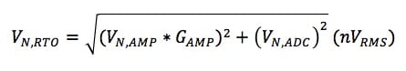
Equation 2
You can now use this output-referred noise equation and transform it into an equivalent input-referred noise source for the system. To accomplish that, first simplify the circuit diagram in Figure 3 to one with an equivalent circuit noise model combining both noise sources into one referred-to-input noise source (VN,RTI). This also simplifies your analysis by allowing you to determine whether the simple signal chain (ADC + amplifier) has enough resolution for your application.
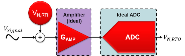
Figure 4. Noiseless components with one total input-referred noise source
To calculate the input-referred noise from the output-referred noise, divide each individual noise term by the circuit gain, GAMP, as shown in Equation 3:
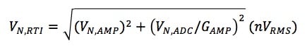
Equation 3
Note the location of the gain term, GAMP, in both Equations 2 and 3. In Equation 2, the amplifier’s noise is proportional to the gain, while in Equation 3 the ADC’s noise is proportional to the inverse of the gain. In either case, given a sufficiently large amplifier gain and comparable amplifier noise, the ADC noise becomes negligible. The resulting input-referred noise is then completely dependent on the amplifier’s noise, given by Equation 4. This is true whether or not the amplifier is integrated into the ADC or is a discrete component.

Equation 4
What if you add additional amplifiers to the signal chain, as in Figure 5? You could add multiple discrete amplifiers or an ADC with an integrated amplifier as well as an external amplifier.
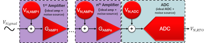
Figure 5. Noiseless amplifiers and noiseless ADC with separate, referred-to-input noise sources
As you did previously, combine all of these noise terms into one input-referred noise source with an equivalent circuit noise model, shown in Figure 6.
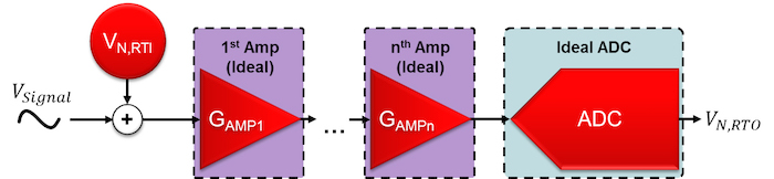
Figure 6. Multiple noiseless amplifiers at the input of an ADC with one total input-referred noise source
You can use Figure 6 and Equations 2 and 3 to help determine the input-referred noise for this extended signal chain with n number of amplifiers, represented by Equation 5:
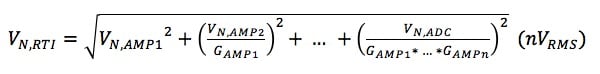
Equation 5
As in the previous example, the new input-referred noise equation depends on the noise contributions of all devices in the signal chain. However, each term is scaled by the inverse of the product of all amplifier gains, leaving only the initial term — the first amplifier’s voltage noise — independent of gain.
Similar to Equation 4, this means that with a large first-stage gain, all other terms in Equation 5 effectively approach zero, leaving the system’s input-referred noise dependent on the noise of the first amplifier only. Therefore, for best performance in both single- and multistage amplifier configurations, choose a low-noise first-stage amplifier with a large gain.
As Equation 4 implies, the effect of this choice is not equal for all ADCs. In fact, you could pair a lower-resolution ADC with a higher-noise amplifier, or use a larger gain and still meet the required system noise performance. Moreover, a higher-resolution ADC might not see any effect from even a modest gain increase.
Let’s analyze these conclusions further by looking at the 16-bit ADS114S08 compared to the 24-bit ADS124S08. These two ADCs have different resolutions but are otherwise identical, including an integrated programmable gain amplifier (PGA) with the same amplifier noise. Their similarities allow you to analyze how the different ADC resolutions affect system noise as gain changes.
Low- vs. High-Resolution ADCs
Figure 7 shows the input-referred noise for both the ADS114S08 and ADS124S08 at gains of 1V/V and 2V/V and for all available data rates. If you choose any data rate — 50SPS, for example — and take the ratio of the input-referred noise at these gains, you will get approximately 2 for both ADCs. In other words, as the gain increases by a factor of 2, the noise simultaneously decreases by a factor of 2. In this case, adding gain improves system noise performance for both the higher- (24-bit) and lower-resolution (16-bit) ADCs.
![Input-referred noise (µVRMS [µVPP ]) tables showing G = 1 and 2V/V – SINC3 filter, AVDD = 3.3V, AVSS = 0V, PGA enabled, global chop disabled and internal 2.5V reference](https://www.allaboutcircuits.com/uploads/articles/Figure_7_Resolving_the_Signal_copy.jpg)
Figure 7. Input-referred noise (µVRMS [µVPP ]) tables showing G = 1 and 2V/V – SINC3 filter, AVDD = 3.3V, AVSS = 0V, PGA enabled, global chop disabled and internal 2.5V reference
Compare that to Figure 8, which shows the same calculations using the highest gains of 64V/V and 128V/V. Here, the lower-resolution ADC has maintained the ratio of 2, while the ratio for the higher-resolution ADC has decreased to approximately 1. In the latter case, increasing gain no longer improves noise performance. What causes this difference?
![Input-referred noise (µVRMS [µVPP ]) tables showing G = 64 and 128 V/V – SINC3 filter, AVDD = 3.3V, AVSS = 0V, PGA enabled, global chop disabled and internal 2.5V reference](https://www.allaboutcircuits.com/uploads/articles/Figure_8_Resolving_the_Signal_copy.jpg)
Figure 8. Input-referred noise (µVRMS [µVPP ]) tables showing G = 64 and 128 V/V – SINC3 filter, AVDD = 3.3V, AVSS = 0V, PGA enabled, global chop disabled and internal 2.5V reference
For the lower-resolution (quantization-noise-dominant) ADC, the constant ratio between the gains results from the high levels of ADC noise compared to amplifier noise. In this case, the condition stated in Equation 4 is not met, as the ADC noise is much larger than the amplifier noise. The ADC noise does decrease each time you increase the gain by a factor of 2, but even at its lowest level (G = 128V/V), the ADC noise still dominates compared to the amplifier noise. Thus, you never actually “see” the amplifier noise in the measurement, making this specific signal chain less dependent on the amplifier’s performance and enabling you to potentially improve the noise performance using larger gain values.
For higher-resolution (thermal-noise-dominant) ADCs, the opposite is true, even though both ADCs use the same amplifier. In this case, the ADC noise is much lower compared to the amplifier noise multiplied by the gain, and therefore meets the condition in Equation 4. As a result, VN,RTI effectively becomes constant, resulting in virtually no change in input-referred noise performance despite increasing gain. In such circumstances amplifier performance is critical, and in many cases using an amplifier results in worse system resolution than a system with no amplifier at all.
To explore these points in more detail, read part 7 of “Resolving the Signal” where I’ll step through a design example that adds different external amplifiers to the input of one high-resolution ADC and compare the system noise performance of each combination.
Key Takeaways
Here is a summary of important points to help better understand how amplifier noise affects delta-sigma ADCs:
- For signal chains with no gain, output-referred noise = input-referred noise.
- Output-referred noise = measured; input-referred noise = calculated.
- Input-referred noise represents the system’s input resolution.
- First-stage amplifier noise dominates the system input-referred noise (assuming similar component noise values and a large first-stage gain).
- Using a high resolution (low-noise) ADC with a noisy amplifier degrades system performance.
- For best noise performance, the first stage is generally configured as a low-noise, small-signal gain amplifier.
Industry Articles are a form of content that allows industry partners to share useful news, messages, and technology with All About Circuits readers in a way editorial content is not well suited to. All Industry Articles are subject to strict editorial guidelines with the intention of offering readers useful news, technical expertise, or stories. The viewpoints and opinions expressed in Industry Articles are those of the partner and not necessarily those of All About Circuits or its writers.


