A single antenna—like a single ear, eye, or audio speaker—works, but combining two or more are better. This works for sending as well as receiving. By sending the same signal from two or more identical antennas in phase with each other, you can boost it, make it extremely directional, or change its shape. This is the concept behind phased arrays, which have found great success in communications, radar, and radio astronomy.
Until now, phased arrays have mostly utilized radio frequencies. Modern nanoscale technology is now allowing researchers to create phased arrays for optical (visible) light. Jie Sun and colleagues fabricated a phased array of 4,096 microscopic antennas on a single silicon chip. This allowed them to shape the output waveform, so they could transmit an image of the MIT logo by combining the light from each tiny antenna in precise ways—something that could not be done with (say) a similar array of LEDs. Potential applications for this research include biomedical imaging, holography, and laser communications.
Phased arrays have had their greatest success at radio wavelengths, where they have been used for radar, AM radio broadcasting, and so forth. (In radio astronomy, the technique goes under the name "aperture synthesis" and led in part to a Nobel Prize for Martin Ryle and Anthony Hewish.) The idea in all these cases is the same: begin with one signal, but multiple identical antennas. By combining the output from each antenna, researchers can selectively create interference patterns, boosting the signal at distance or canceling it out entirely where it might overlap with another signal.
Radio waves have relatively large wavelengths and consequently require large antennas. This makes phased arrays that utilize radio wavelengths pricey, leading researchers to consider other portions of the electromagnetic spectrum. Although there are cheap options for working with visible light, it has the opposite problem as radio: its wavelengths are very small, and its antennas must be fabricated roughly on the same scale—400 to 700 nanometers (nm), or 0.0004 to 0.0007 millimeters.
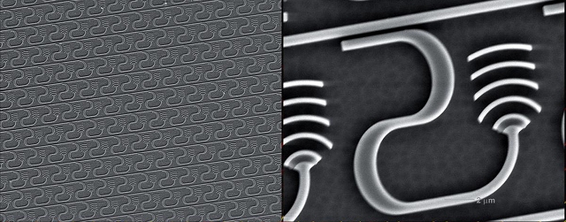
The current experiment drew on earlier work, which created lines of nanophotonic phased arrays (NPAs) and small two-dimensional chips. The researchers fabricated a 64×64 "pixel" array of identical square antennas, each 9 microns (0.009mm) on the side. The entire array was formed out of silicon, with connecting silicon "wires" made by the same process. (The "wires" were actually waveguides, microscopic channels that shape the light passing along them in particular ways.) The researchers used a standard fabrication technique developed for complementary metal-oxide semiconductor (CMOS) chips, commonly used in consumer electronics.
Each antenna could emit across several nanometers of wavelength, allowing for multi-color transmission. A single laser fed the input to the entire NPA using a fiber optic cable. By altering the phase of the light—where the crests and troughs of the light wave occur—in the antennas, the researchers exerted tight control over the pattern that appeared at a distant detector.
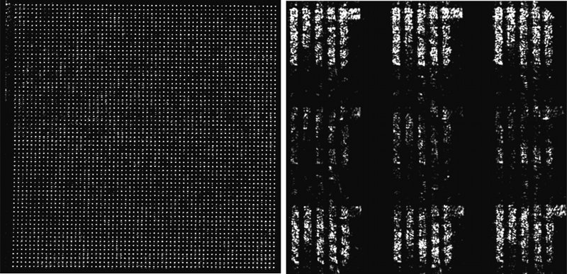
With 4,096 phased antennas packed into a square just 0.8 millimeters across, the array could do tricks unavailable to its radio-frequency cousins. To demonstrate this, the researchers controlled the emission from the NPA to generate the MIT (Massachusetts Institute of Technology) logo. That pattern is sufficiently detailed as to require many antennas to produce, so while the specific choice was somewhat irrelevant (if loyal to many of the researchers' affiliation), it demonstrated the capabilities of the array effectively.
The NPA demonstrated a powerful proof of principle, one that could have immediate application in optical systems that require tight control over the shape of light emission. Future nanoscale devices fabricated along these lines could exploit laser technology for optical-band communication, holography, medical imaging—and new uses we haven't yet conceived.
Nature, 2013. DOI: 10.1038/nature11727 (About DOIs).
reader comments
18