

Update to the original story post-funding and DARPA contact
When Rex Computing CEO, Thomas Sohmers, was working with embedded computing systems for military applications at MIT at age 13, his thoughts turned to much larger scale systems. For exascale-class computing, he realized there were many lessons to be carried over from embedded computing that could potentially have an impact on the toughest challenges that lie ahead—balancing the performance demands with overall power efficiency and scalability of both the hardware and software.
The result of his research is an up and coming chip called Neo, which brings to bear a new architecture, instruction set, and core design that scraps a great deal of what Sohmers deems unnecessary about current cache architecture, snaps in a new interconnect, and if his assumptions are correct, can do this in a power envelope and performance target that goes beyond the current Department of Energy requirements for exascale computing goals, which they hope to realize in the 2020 to 2023 timeframe.
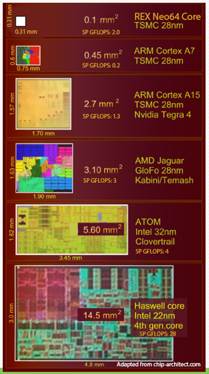 Sohmers says that the national labs are already expressing early interest in the 64-bit Neo cores, which are 1/145 the size of a fourth generation Haswell core and 1/27 the size of a 32-bit ARM Cortex A-15. He expects to deliver a 256 core chip by the end of 2016 at the earliest using a 28 nanometer process, which will offer 65 gigaflops per watt. Successive generations will use 10 nanometer or 7 nanometer processes as those roll out. “Current proposals for exascale in 2022 are for 20 megawatts, but it’s definitely possible to do better than that within five years,” he noted.
But how is it possible to see the required performance within these kinds of power constraints? A solid place to start is at the current bottlenecks and one in particular that captured his attention. The inherent inefficiencies of cache.
“Caches and virtual memory as they are currently implemented are some of the worst design decisions that have ever been made,” Sohmers boldly told a room of HPC-focused attendees at the Open Compute Summit this week. “A lot of people are thinking about the HPC problem incorrectly. Caches are great when you’re thinking of things from a pure memory and latency point, but as time went on, so many extra features were layered into the cache systems, especially virtual memory, that while making the programmers lives easier (especially before compilers), it added a lot of new inefficiencies.”
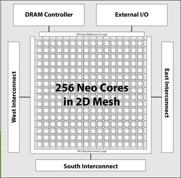 Neo is a 256 core MIMD processor that will offer 256 gigaflops at double precision, 512 for single precision that is able to multitask remarkably well. The concept is that for every cycle, there is an ALU operation, a double-precision floating operation, a load store from the local memory to registers (or vice versa) and a DMA operation—all happening at once to push the pipeline.
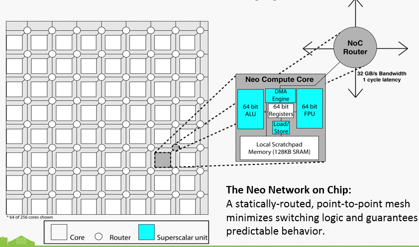
To do this, there is what Sohmers calls a “scatchpad” that is a physically addressed SRAM block. In other words, there is no virtual memory translation happening, which in theory, will significantly cut latency (and hence boost performance and efficiency). This means that there is one cycle to address the SRAM, so “this saves half the power right off the bat just by getting rid of address translation from virtual memory.”
At the core level it manages all of this by using quad-issue VLIW, although the system is functionally superscalar and eschews doing some of the new things like using variable lengths where one can change the number of instructions. “The key is to have a full quad-issue pipeline that is kept full at all times and doing an operation every single cycle.” To do that, the design takes the complexity out of the instruction decoder, which saves around 5-10 percent area on the core.
When you think about how this is laid out on a chip, let’s say that core 0 has its own 128 KB of SRAM and the first 128 KB of that address space. When we go to core 1 (for example), it is just a continuation of that address space. When core 1 needs to access something in another core, it uses a DMA operation, takes one cycle to get there, and can do an operation there. The key is that we can guarantee the number of cycles it takes to go from any core—so while a core can do a floating point operation, use the ALU and do load store, it can also be doing DMA every cycle to every other piece of memory on the chip or every other interconnected chip.”
Of course, central to all of this is that interconnect, which Sohmers and his partners have designed. There are three bi-directional interconnects (six interfaces), which provide a parallel point-to-point interface that allows up to 48 GB/s per direction (so 96 GB/s bi-directional), leading to a total aggregate bandwidth of 288 GB/s per chip. The idea for future exascale systems built on these chips is to set them up in a grid and be able to communicate free from the constraints of PCI or NVlink. In fact, Sohmers says he anticipates a 2X improvement over PCI and 4X over NVlink.
Even with all of the potential for performance and efficiency, however, without the ability for programmers to port and make use of Neo, all will be in vain. And while power and performance are key considerations for future exascale systems the biggest challenge of all, as some might argue, is the massive parallel programming challenge ahead.
Sohmers says that in his observations of how other chip upstarts have rolled into the game, they expect the software to follow after the hardware is refined and ready. There has to be a “holistic approach where the hardware and software are considered together” he argued, pointing to work his co-founder is doing to make sure the ISA and portability are produced in lockstep with the chip. “The idea is to make it programmable and have an easy way to port over to our architecture. It’s a VLIW approach, which is not that different from existing architectures beyond the cache. So porting will be reliant on predicting where the memory will be and placing it on the grid.” We will follow up to explore the software challenges in a coming article, but in essence, Rex Computing plans to open its reference architecture and begin pushing development tools out to early testers as early as next year.
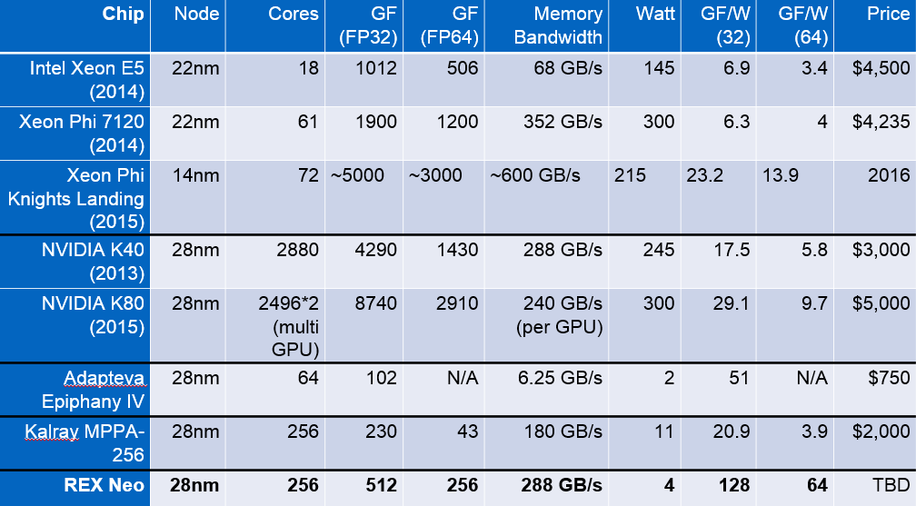
As we noted, Rex Computing was presenting at Open Compute Summit this week for an audience of a special HPC working group within the project. He says that opening the architecture is critical to add new thinking and possibilities in semiconductors, especially in the context of the current price/performance paradigms of the current HPC offerings, a comparison of which he offers below.
Aside from the hardware and software plans for the near term, Rex Computing is looking at a few other areas, including a new project called Unum, which seeks to reduce the number of bits that are moved down to 29 for the same amount of work. They are also exploring how they might wrap a 2D mesh from each side of the system, which Sohmers says is something they’ve figured out a “trick” to do, even if it’s still loaded with wires.
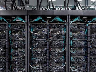
He showed how Neo might fit into an Open Compute system using Penguin’s 1U box outfitted with 16 of the Rex Computing chips.
“Based on the other component costs, including DRAM, the efficiencies at rack scale as demonstrated here are within the exascale power limits. A single one of these 1U tall sleds is around 80 watts with the compute portion consuming 50 to 80 of those units.
These are big claims for a…okay, we won’t call him a kid. But as Sohmers openly said to his HPC-centric audience this week, his youth is an advantage. He is clearly excited, giddy even, when talking about Seymour Cray and the various incremental developments in supercomputing architectures. But he says that not having made the mistakes of those previous generations and approaching large-scale computing with an entirely fresh perspective is exactly what is needed when challenges like actual power-efficient exascale computing are at the fore.


Livermore Converges A Slew Of New Ideas For Exascale Storage
There are a lot of new technologies that are available now or are going to be available shortly that have the potential to radically change the compute, memory, and storage hierarchies in systems. It is a great time to be a system architect, given all of the component and interconnect …
So, You Think You Can Design A 20 Exaflops Supercomputer?
UPDATED* Perhaps Janet Jackson should be the official spokesperson of the supercomputing industry. The US Department of Energy has a single 2 exaflops system up and running – well, most of it anyway – and that of course is the “Frontier” system at Oak Ridge National Laboratory and two more …

Going Beyond Exascale Computing
One thing is certain: The explosion of data creation in our society will continue as far as pundits and anyone else can forecast. In response, there is an insatiable demand for more advanced high performance computing to make this data useful. The IT industry has been pushing to new levels …
How does a 13 year old obtains a clearance to work on military application? Just curious…
Not all military projects are classified. And if it was then maybe he was cleared.
Accolades to the writer of this article.. !!
Nicole I have been waiting for this compute technology to come along. I would say that a marriage of this new compute technology with Resistive RAM would take this the Exasacle compute technology to Zettascale.
https://www.linkedin.com/pulse/20140711173826-3543789-bigger-than-google?trk=prof-post
Simply put, Resistive RAM is the first memory technology that will allow a marriage between compute and high density high speed memory on the same die. RRAM costs 1 Femto amp of power to engage a bit flip. Recent developments have removed the obstacle which would have prevented stacking & bank switching of RRAM. Bank switching is an old technique which allows many layers of RRAM to be multiplexed to achieve current DDR Speeds in Terabyte scale. RRAM will replace every memory subsystem placing all memory on the CPU die. Alone this technology would be able to remove memory bottle necks so that Exascale could be achieved within a year. Couple this with the Neo Chip technology and we have would have incredible speed enhancements.
Moving right along, with RRAM on die.. no longer would the Neo chip need to be a 2D mesh networked processor. I could easily become a 3D meshed network on a chip with unrivaled capabilities.
A marriage of RRAM and current APU technologies we could see the shrining of a 1U 4 processor high density HPC server reduced to the size of a credit card. 1U server is 17.7″ W x 1.75″ T x ~28″ D. One 42U data center cabinet with 3,000 to 5,000 credit card sized servers could replace 38-62 cabinets loaded with standard 1U server kits.
An impressive architecture and packaging to be sure.
But I need to observe that virtual memory is not some old relic of computing days gone by. As a few reminders of the reasons virtual addressing exists:
o If a system is going to support multiple applications each associated with a process and those processes require the security advantages of data isolation between processes, the system needs virtual addressing.
o If the size of the system’s data exceeds the available memory and accesses to the larger data are expected to transparent to the programmer, the system needs virtual addressing.
o If some sets of applications are allowed to access data in memory not available to others, the system needs virtual addressing.
o If such a system will be used “in the cloud” with its expectation that there can be multiple OS instances per system, cross-OS isolation relies on virtual addressing.
Of course, if the applications using this system …
o Intend to take over the entire set of processors and memory,
o Are willing to manually map any data not in memory into the memory’s address space,
o Trust each other implicitly,
then, yes, jettisoning virtual addressing seems like a quite reasonable trade-off of chip real estate.
So when folks talk about exascale computing, to which model are they referring? And, yes, the answer can be both, just as long as the users and software base are very aware of the distinction.
Might I also add that – just as Mr. Sohmers – the relatively older codger writing this post (and I suspect many in HPC land) also remain excited and even giddy concerning near future computer architectures.
Welcome to our new digs, Mark….
Each core address virtual processing and segregation. Its just a different way of looking at virtualization.
I’m thinking that this chip would be a perfect addition to USB Storage for additional high security encryption. I hope Rex Computing CEO, Thomas Sohmers, uses this information to gain a foothold in the encryption market and notoriety that comes forthwith. I am sure the Sandisk’s of the world would love a solution like this.
What the article does not discuss–but I suspect Rex Computing has thought of–is how you bridge the different speeds of DRAM and CPU. This is one of the biggest reasons for cache memory.
If your memory bus clock is 1.0 GHz and you are going to DMA read at row and column address A on the first clock cycle and DMA write at address row and column B on the second clock cycle and DMA read at address row and column C on the third clock cycle, you need something much faster than DDR4 because despite the impressive bandwidth of DDR4 memory, you cannot switch between reads, writes, rows and columns in single bus clock cycles. Cache memory helps eliminate stalls by giving you have multiple layers of buffers between DRAM and CPU.
Does the Neo CPU keep power usage low by spending most of its time in stall? Probably not, but I am not sure what the solution is.
Maybe inversing the layers and have the capacitance loopback into the inductive phase could improve the timings?
It sounds interesting especially with the unum concept for better numerical accuracy. Maybe they can go for a golden price tag in the exascale market, but I don’t think decision makers would be so easy to convince. They should think about selling a 16 core version for a buck it they think such an arrangement would be more powerful than an ARM 64 bit chip. It’s a tough market place, sure you can sell a few 10’s of thousands to the curious, high volume sales are really difficult.
Of course, I agree that central to all of this is that interconnect … which was not dealt with adequately in the article. I mean, we know all about ALU, FPU, Cache, RAM etc. issues, but talking about exascale, it is all about that interconnect, from both hardware and software point of view. The issue has been festering for two decades, isn’t time to concentrate on the that?
Inmos Transputer
I’m a microprocessor architect, so know where this is coming from. There’s nothing new here – if this was a successful technique it would already be what everyone is using, since there’s one of these “redesign everything for efficiency with tiny cores” about every six months. VLIW beyond a few not-too wide Intel instructions isn’t a success for a reason, it’s all about compilers that can only do so well and numerical software that’s difficult to modify for performance. And the 4 watt power numbers in this slide are an outright marketing tale – a 288 GB/s memory interface is about 12 watts assuming cores are 0 watts. At best this architecture will get a couple of applications to port software and then lager for a few years before dying.
this looks like a clone of Ephiphany architecture
https://arxiv.org/pdf/1610.01832v1.pdf