The idea of substituting electrons with photons in computing has led to a variety of approaches for achieving the promise of speed-of-light computing. Not many of these schemes, however, have involved devices in which electronic currents are optically switched and amplified only by light and without the need for an electronic gate.
Now a team of researchers at Korea University has jumped into this largely untouched field with a nanowire-based transistor in which photons control nanowire logic gates. The researchers—who have dubbed their device a photon-triggered nanowire transistor (PTNT)—believe that their results show a way forward in using photons in logic gates, leading to ultracompact nanoprocessors and nanoscale photodetectors for high-resolution imaging.
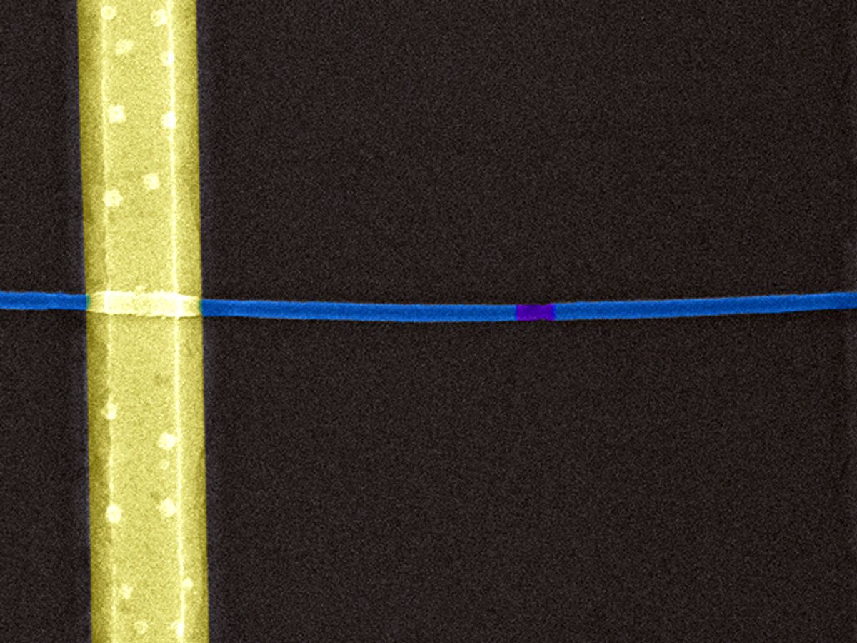
In work described in the journal Nature Nanotechnology, the Korean researchers fabricated the PTNTs from semiconductor nanowires that are synthesized to have long crystalline silicon segments connected by short porous silicon segments. Electrical contacts were made at either end of the nanowire on the crystalline portion.
These porous silicon segments in the middle of the nanowires act as a reservoir of trapped electrons that effectively inhibits current across the electrode, creating the “off” state of the transistor. But because the porous silicon is very sensitive to light, the current can be controlled—turned on and off—by pumping light into it.
When the light is hitting the porous silicon, those trappped electrons are excited into a higher energy state to the point where they get diffused through the nanowire enabling a current across the electrodes. This creates the “on” state of the transistor. This all leads to the porous silicon segments serving as a high on/off current ratio field-effect transistor. The ratio reached 106, which is comparable to the best values of previous silicon nanowires.
Hong-Gyu Park, a professor at Korea University, who co-authored the research, told IEEE Spectrum he believes that the PTNT device they have developed possesses advantages of both photonic and electronic devices. In the photon-triggered transistors—which are similar in size to other nanoscale electronic transistors—the electric currents are switched and amplified just like conventional all-electronic transistors.
Park and his colleagues have also synthesized more complex structures containing two porous silicon segments along the nanowire that can be triggered using two independent optical input signals. By using localized pump lasers as inputs and the current or voltage as output, the researchers were able to demonstrate photon-triggered logic gates including AND, OR, and NAND gates, which are fundamental building blocks of modern computer processing.
While the initial results are encouraging, the processing used to make the porous silicon segments—metal-assisted chemical etching—needs improving. This processs lead to nanowires that have rougher surfaces than typical bottom-up grown nanowires, resulting in a higher device resistance. Park says that they will need to make smoother nanowire surfaces to improve device performance.
Nonetheless Park believes that PTNT devices offer an innovative approach towards multifunctional device applications, such as programmable logic elements and ultrasensitive detectors.
“We expect in the future to scale-up the production of photon-triggered transistors through the mass production of silicon nanowires with porous silicon segments,” he says.
Dexter Johnson is a contributing editor at IEEE Spectrum, with a focus on nanotechnology.


