Since it was first unveiled, we've learned bits and pieces about the hardware inside Microsoft's HoloLens augmented reality headset. But Microsoft's custom Holographic Processing Unit (HPU) has always posed something of a mystery. At Hot Chips this week, the company finally shed a little light on what its special chip is doing.
Ever since we first used HoloLens, we knew that it had some special hardware. Our first units weren't the sleek all-in-one devices that are now available to developers and corporations for $3,000. Instead, each of our devices had a bulky chest-mounted unit that contained an FPGA (a kind of chip that can be rewired on-the-fly to change its behavior), fans to keep it cool, and an umbilical cord to provide power.
That FPGA was the precursor to the HPU that the HoloLens headsets now contain. The HPU integrates data from the HoloLens's sensors (accelerometers to detect motion and a Kinect-like camera system to detect depth). The chip uses those sensors to recognize gestures, maintain a map of the environment, and ensure that virtual 3D objects retain their position in the real world.
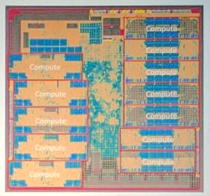
The HPU contains 24 Tensilica DSP (digital signal processor) cores. Tensilica DSPs pop up in a few different places; for example, AMD has used them for its TrueAudio audio processing and its hardware-accelerated video codecs. Other companies have built Wi-Fi chips around the Tensilica DSP, too.
Microsoft evaluated off-the-shelf vision-processing chips, but the company couldn't find anything that had the right combination of performance, latency, and power usage. So the company decided to go the custom route.
Cadence, which owns Tensilica, licenses Tensilica cores, providing companies with all the information they need to build their own chips. The cores are designed to be readily extended to allow custom instructions and capabilities to be added, with Cadence providing various customization tools; this sets Tensilica apart from other licensed designs, such as those from ARM, which require expensive licenses to enable comparable custom design work.
Microsoft added a number of custom instructions to the cores (variously reported as 300 by EE Times, 10 by The Register). These instructions provide dense encodings of the various mathematical operations that the HPU needs to perform, with a mix of fixed function and general purpose hardware to perform the actual computations. General purpose elements are preferred, but some operations need fixed function hardware to meet the company's performance goals.
The cores share 8MB of SRAM cache and 1GB of DDR3 RAM integrated onto the package. The HPU has both PCIe and serial connectivity to the sensors and to the HoloLens's Atom processor. In total, there are about 65 million logic gates in the 12×12mm package, and it's all built on TSMC's 28nm process.
Microsoft says that the HPU can perform about one trillion floating point operations per second and is 200 times faster than a pure software equivalent. The whole chip draws under 10W, as compared to the 4W used by the Intel Cherry Trail Atom SoC that provides the HoloLens's CPU and GPU. The HPU provides the CPU with highly processed "cooked" data which is in turn exposed to the 3D programs running on the headset.
The design has also been future-proofed to some degree. At the moment, the HPU operates at no more than 50 percent of its capacity, with plenty of compute cycles still available. Someday in the future, Redmond should be able to add more sensor data, more complex algorithms, richer gesture recognition, or some combination of these without requiring the HPU to be completely redesigned.
reader comments
68