The first full-fat GPU based on Nvidia's all-new Pascal architecture is here. And while the Tesla P100 is aimed at professionals and deep learning systems rather than consumers, if consumer Pascal GPUs are anything like it—and there's a very good chance they will be—gamers and enthusiasts alike are going to see a monumental boost in performance.
The Tesla P100 is the first full-size Nvidia GPU based on the TSMC 16nm FinFET manufacturing process—like AMD, Nvidia has been stuck using an older 28nm process since 2012—and the first to feature the second generation of High Bandwidth Memory (HBM2). Samsung began mass production of faster and higher capacity HBM2 memory back in January. While recent rumours suggested that both Nvidia and AMD wouldn't use HMB2 this year due to it being prohibitively expensive—indeed, AMD's recent roadmap suggests that its new Polaris GPUs won't use HBM2—Nvidia has at least taken the leap with its professional line of GPUs.
The result of the P100's more efficient manufacturing process, architecture upgrades, and HBM2 is a big boost in performance over Nvidia's current performance champs like the Maxwell-based Tesla M40 and the Titan X/Quadro M6000. Nvidia says the P100 reaches 21.2 teraflops of half-precision (FP16) floating point performance, 10.6 teraflops of single precision (FP32), and 5.3 teraflops (1/2 rate) of double precision. By comparison, the Titan X and Tesla M40 offer just 7 teraflops of single precision floating point performance.
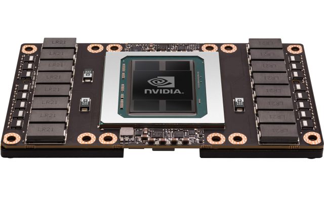
Memory bandwidth more than doubles over the Titan X to 720GB/s thanks to the wider 4096-bit memory bus, while capacity goes up to 16GB. Interestingly, the Tesla P100 isn't even a fully enabled version of Pascal; it's based on the company's new GP100 GPU, with 56 of its 60 streaming multiprocessors (SM) enabled. The GP100 die, with a surface area of 610 square millimetres, is roughly the same size as the GM200 Titan X. Rather than shrink down the die thanks to the smaller 16nm process, Nvidia has instead chosen to simply fill the same space up with a lot more transistors—15.3 billion of them to be precise—almost doubling that of the top-end GM200 Maxwell chip.
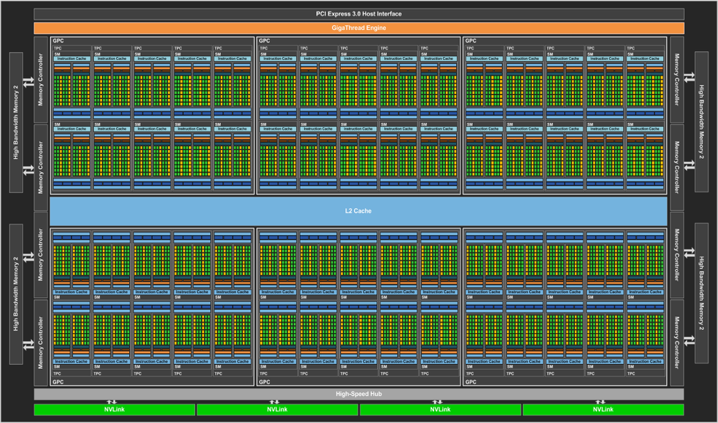
While Nvidia hasn't unveiled all the underlying details of the Pascal architecture just yet, there are some interesting tidbits to be gleaned from the initial info. There's a core clock of 1328MHz and a boost clock of 1480MHz—both much higher than Maxwell-based GPUs—along with a 300W TDP. Pascal features 64 FP32 CUDA cores per SM, compared with 128 on Maxwell, with each of those SMs also containing 32 FP64 CUDA cores. That results in the 1/2 rate performance of double precision floating point. Pascal is also able to pack two FP16 operations inside a single FP32 CUDA core. The HBM2 memory is laid out in four 4GB stacks, each with a 1024-bit width for a total 4096-bit memory bus.
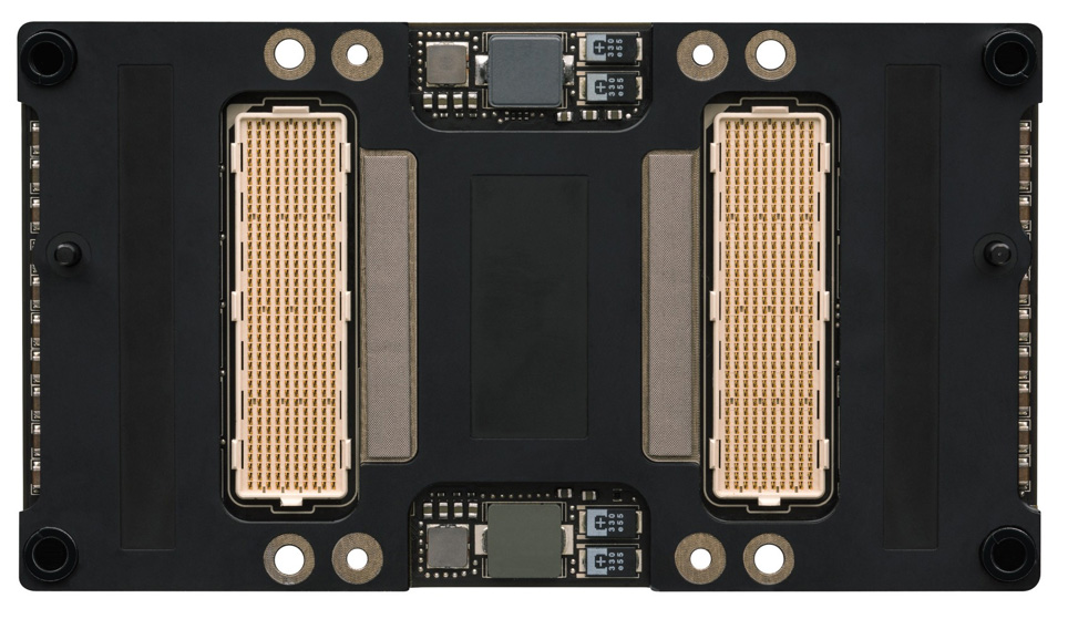
The P100 also supports NVLink, a proprietary interconnect announced way back in 2014 that allows multiple GPUs to connect directly to each other or supporting CPUs at a much higher bandwidth than currently offered by PCI Express 3.0. It also supports up to eight GPU connections, rather than the four of PCIe and SLI.
"GPUs have fast but small memories, and CPUs have large but slow memories," Nvidia CEO Jen-Hsun Huang said back in 2014, when NVLink was originally announced. "Accelerated computing applications typically move data from the network or disk storage to CPU memory and then copy the data to GPU memory before it can be crunched by the GPU. With NVLink, the data moves between the CPU memory and GPU memory at much faster speeds, making GPU-accelerated applications run much faster."
Huang also teased at the time that systems packing Pascal graphics would wind up being 10 times faster than Maxwell-based systems—but at GTC 2016, as he unveiled the P100, he upped the ante, saying that certain tasks will see a 12-fold increase in speed. A task that completes in 25 hours on a Maxwell-accelerated PC may take just two hours on a Pascal system, he claimed.
Launching alongside the Tesla P100 is Nvidia's DGX-1 Deep Learning System. The DGX-1 features eight Tesla GP100 GPU cards providing 170 teraflops of half-precision performance from its 28,672 CUDA cores. The DGX-100 also features two 16-core Intel Xeon E5-2698 v3 2.3GHz CPUs, 512GB of DDR4 RAM, 4x 1.92TB SSD RAID, dual 10GbE, 4x InfiniBand EDR network ports, and requires a maximum of 3200W of power. It'll cost a mere $129,000 (~£103,000) when it launches in June. Those after a P100 in other types of servers will have to wait a little longer, with cards expected to reach systems in 2017, likely due to binning and HBM2 manufacturing constraints.
Those same restraints may mean that consumer graphics cards based on Pascal, such as the rumoured GTX 1080 and 1080Ti, are more likely to feature good old GDDR5, or perhaps even GDDR5X, a higher bandwidth version of the technology intended to compete with HBM. Even if they do, the innate processing grunt of Pascal will still make a huge difference to performance in 3D applications like video games and virtual reality. The FP32 performance—which is the most important for games—is still 43 percent higher in the Pascal GP100 than the Maxwell GM200.
With Pascal now at least partly outed thanks to the P100, expect Nvidia to drop details on the consumer cards soon—probably before E3 in mid-June.
reader comments
100